
PN Junction (Silicon) Diode Characteristics

LEARNING OUT COMES
To observe and draw the Forward and Reverse bias V-I Characteristics of a P-N Junction diode.
EQUIPMENT AND MATERIALS
1. DC Regulated Power supply (0-30v)
2. P-N Diode IN4007
3. Resistor 1kΩ
4. Ammeters (0-200mA, 0-500mA)
5. Voltmeter (0-20v)
6. Bread board
7. Connecting wires
DESCRIPTION
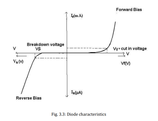
A p-n junction diode conducts only in one direction. The V-I characteristics of the diode are curve between voltage across the diode and current through the diode. When external voltage is zero, circuit is open and the potential barrier does not allow the current to flow. Therefore, the circuit current is zero. When P-type (Anode is connected to +ve terminal and n- type (cathode) is connected to ve terminal of the supply voltage, is known as forward bias. The potential barrier is reduced when diode is in the forward biased condition. At some forward voltage, the potential barrier altogether eliminated and current starts flowing through the diode and also in the circuit. The diode is said to be in ON state. The current increases with increasing forward voltage.
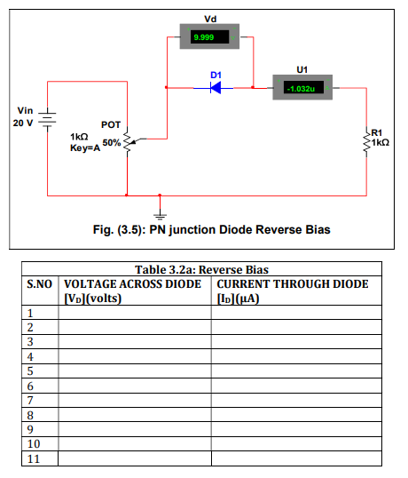
When N-type (cathode) is connected to +ve terminal and P-type (Anode) is connected ve terminal of the supply voltage is known as reverse bias and the potential barrier across the junction increases. Therefore, the junction resistance becomes very high and a very small current (reverse saturation current) flows in the circuit. The diode is said to be in OFF state. The reverse bias current due to minority charge carriers
PROCEDURE
FORWARD BIAS:
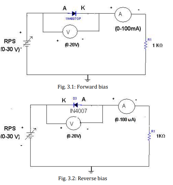
1. Connect the circuit as per the circuit diagram shown in Fig. 3.1
2. For forward bias, the (Regulated Power supply) RPS +ve is connected to the anode of the diode and RPS ve is connected to the cathode of the diode
3. Switch on the power supply and increase the input voltage (supply voltage) such that voltage across diode increases in steps of 0.1v
4. Note down the corresponding current flowing through the diode and voltage across the diode for each and every step of the input voltage
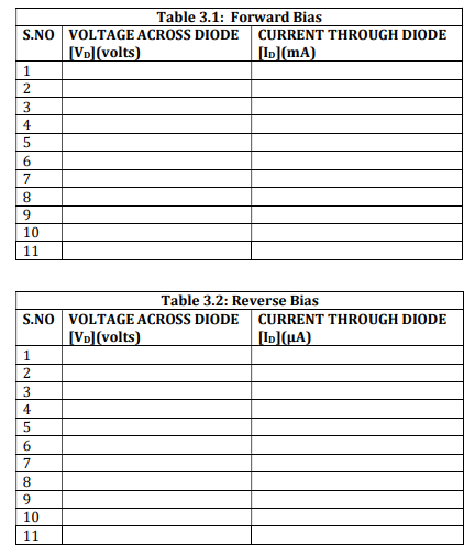
5. The reading of voltage and current are tabulated in Table 3.1..
6. Graph is plotted between voltage and current as shown in the Fig. 3.3 forward bias curve.
REVERSE BIAS:
1. Connections are made as per the circuit diagram shown in Fig. 3.2
2. For reverse bias, the RPS +ve is connected to the cathode of the diode and RPS ve is connected to the anode of the diode.
3. Switch on the power supply and increase the input voltage (supply voltage) such that voltage across diode increases in steps of 1v upto 5v and then in steps of 5v upto 30v
4. Note down the corresponding current flowing through the diode and voltage across the diode for each and every step of the input voltage.
5. The readings of voltage and current are tabulated in Table 3.2
6. Graph is plotted between voltage and current as shown in the Fig. 3.3 reverse bias curve.
EXPECTED RESPONSE:
OBSERVATION AND CALCULATIONS
RESULT& CONCLUSION
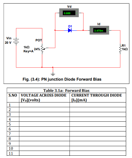
Multisim Simulation:
PN Junction (Silicon) Diode Characteristics نواتج التعلم ملاحظة ورسم خصائص الجهد–التيار (V–I) لدايود الوصلة الثنائية P–N في حالتي الانحياز الأمامي والانحياز العكسي. الأجهزة والمواد المستخدمة مزود طاقة مستمر منظم (0–30 فولت)دايود وصلة ثنائية (P–N) من النوع 1N4007مقاومة 1 كيلو أوم (1 kΩ)أميتران بمدى 0–200 مللي أمبير و0–500 مللي أمبيرفولتميتر بمدى 0–20 فولتلوحة تجارب (Breadboard)أسلاك توصيل…
الفصل الأول دوائر التقويم (دوائر مزود القدرة) تتكون دائرة مزود القدرة من: أ- المحول (Transformer) ب- المقوم (Rectifier) ج- دائرة التنعيم (Smoothing Circuit) المحول (Transformer) يوفر المحول الجهد المطلوب على الملف الثانوي. المقوم (Rectifier) يقوم المقوم بتحويل التيار المتردد (AC) إلى تيار مستمر نابض (Pulsating DC). في هذه التجربة يُستخدم مقوم جسر (Bridge Rectifier)،…
LEARNING OUT COMES A) To observe and draw the static characteristics of a Zener diode B) To find the regulation characteristics of a given Zener diode EQUIPMENT AND MATER IALS 1. Zener diode 2. Regulated Power Supply (0-30v) 3. Voltmeter (0-20v) 4. Ammeter (0-100mA) 5. Resistor (1kΩ) 6. Bread Board 7. Connecting wires DESCRIPTION A…
PN Junction (Silicon) DiodeCharacteristics مرحباً بكم في هذا الدليل العملي المخصص لطلاب الهندسة الإلكترونية والاتصالات والحاسب الآلي. سنقوم اليوم بشرح تفصيلي وإرشادي لتنفيذ تجربة دراسة منحنى الخواص للتيار والجهد (V-I Characteristics) لدايود السيليكون في حالتي الانحياز الأمامي والعكسي . الأهداف التعليمية من التجربة (Learning Outcomes) الأجهزة والمواد المستخدمة (Equipment & Materials) لإعداد هذه التجربة في…
LEARNING OUT COMES A) To observe and draw the static characteristics of a Zener diodeB) To find the regulation characteristics of a given Zener diode نواتج التعلم (Learning Outcomes) أ) ملاحظة ورسم الخصائص الاستاتيكية (السكونية) لدايود زينر (Zener Diode). ب) إيجاد خصائص تنظيم الجهد (Voltage Regulation Characteristics) لدايود زينر المعطى. EQUIPMENT AND MATERIAL 1. Zener…